- 您现在的位置:买卖IC网 > Sheet目录484 > NOII5SM1300A-QDC (ON Semiconductor)SENSOR IMAGE MONO CMOS 84-LCC
�� �
�
�NOII5SM1300A�
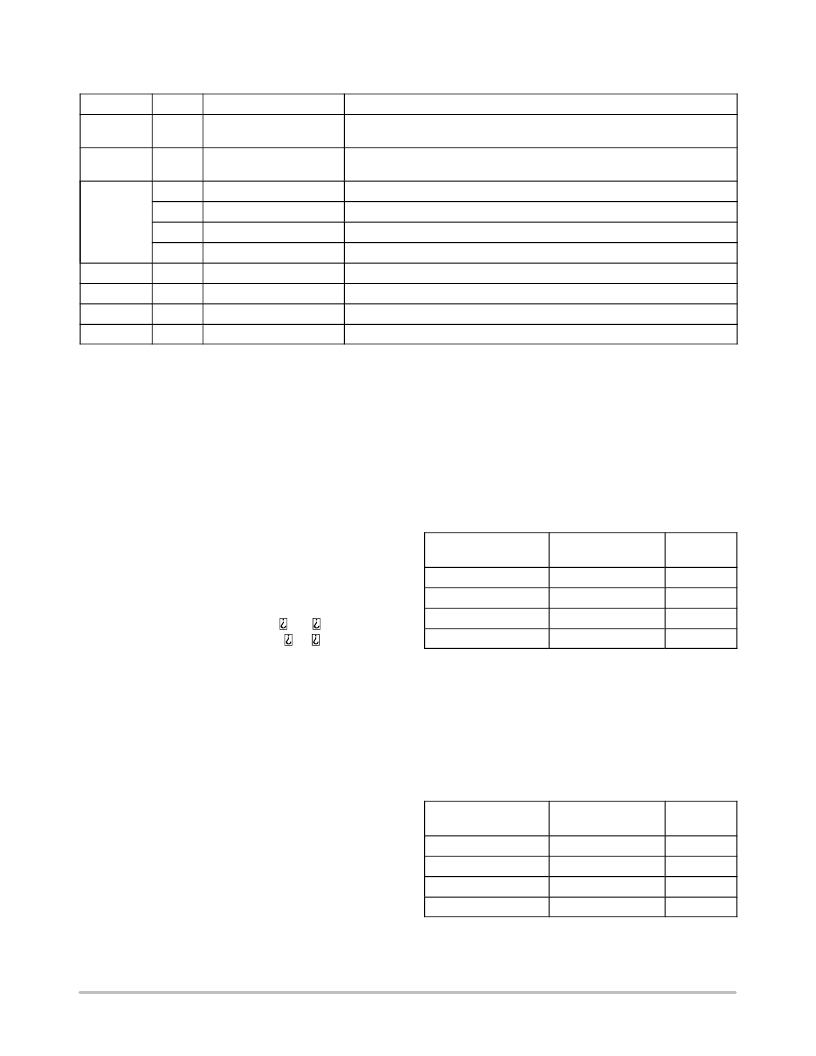
�Table� 15.� INTERNAL� REGISTERS�
�8� (1000)�
�9� (1001)�
�10� (1010)�
�11� (1011)�
�12� (1100)�
�13� (1101)�
�14� (1110)�
�15� (1111)�
�6�
�6:0�
�6:0�
�2:0�
�0�
�1�
�2�
�STANDBY�
�DACRAW_REG�
�DACFINE_REG�
�ADC� register�
�TRISTATE_OUT�
�GAMMA�
�BIT_INV�
�Reserved�
�Reserved�
�Reserved�
�Reserved�
�0� =� Amplifier� in� standby� mode�
�Amplifier� DAC� raw� offset�
�Default� value� <6:0>:� ‘1000000’�
�Amplifier� DAC� fine� offset�
�Default� value� <6:0>:� ‘1000000’�
�Default� value� <2:0>:� ‘011’�
�0� =� Output� bus� in� tri-state�
�0� =� Gamma-correction� on�
�1� =� Bit� inversion� on� output� bus�
�Detailed� Description� of� Internal� Registers�
�Sequencer� register� (7:0)�
�1.� Shutter� type� (bit� 0)�
�The� IBIS5-1300� image� sensor� has� two� shutter� types:�
�0� =� synchronous� shutter�
�1� =� rolling� shutter�
�2.� Output� amplifier� calibration� (bits� 1� and� 2)�
�Bits� FRAME_CAL_MODE� and�
�LINE_CAL_MODE� define� the� calibration� mode� of� the�
�output� amplifier.�
�During� every� row-blanking� period,� a� calibration� is�
�done� of� the� output� amplifier.� There� are� two� calibration�
�modes.� The� FAST� mode� (0)� forces� a� calibration� in� one�
�combined� into� one� pixel� stream� at� the� same� frequency�
�as� SYS_CLOCK.�
�Use� the� bits� GRAN_SS_SEQ_MSB� (bit� 7)� and�
�GRAN_SS_SEQ_LSB� (bit� 6)� to� program� the� clock� that�
�drives� the� ‘snapshot’� or� synchronous� shutter� sequencer.�
�This� way� the� integration� time� in� synchronous� shutter�
�mode� is� a� multiple� of� 32,� 64,� 128,� or� 256� times� the�
�system� clock� period.� To� overcome� global� reset� issues,�
�use� the� longest� SS� granularity� (bits� 6� and� 7� set� to� ‘1’).�
�Table� 16.� SS� SEQUENCER� CLOCK� GRANULARITIES�
�GRAN_SS_SEQ_MSB/� SS-Sequencer� Clock� Integration�
�LSB� Time� Step� [1]�
�cycle� but� is� not� so� accurate� and� suffers� from� KTC� noise.�
�The� SLOW� mode� (1)� only� makes� incremental�
�adjustments� and� is� noise� free.�
�Approximately� 200� or� more� slow� calibrations�
�have� the� same� effect� as� one� fast� calibration.�
�00�
�01�
�10�
�11�
�32� x� SYS_CLOCK�
�64� x� SYS_CLOCK�
�128� x� SYS_CLOCK�
�256� x� SYS_CLOCK�
�800� ns�
�1.6� m� s�
�3.2� m� s�
�6.4� m� s�
�Different� calibration� modes� are� set� at� the� beginning� of�
�the� frame� (FRAME_CAL_MODE� bit)� and� for� every�
�subsequent� line� that� is� read� (LINE_CAL_MODE� bit).�
�The� Y_START� input� defines� the� beginning� of� a� frame,�
�Y_CLOCK� defines� the� beginning� of� a� new� row.�
�3.� Continuous� charge� (bit� 3)�
�Some� applications� may� require� the� use� continuous�
�charging� of� the� pixel� columns� instead� of� a� pre-charge� on�
�every� line� sample� operation.�
�Setting� bit� CONT_CHARGE� to� ‘1’� activates� this�
�function.� The� resistor� connected� to� pin� PC_CMD�
�controls� the� current� level� on� every� pixel� column.�
�4.� Internal� clock� granularities� (bits� 4,� 5,� 6� and� 7)�
�1.� Using� a� SYS_CLOCK� of� 40� MHz� (25� ns� period).�
�The� clock� that� drives� the� X-sequencer� is� a� multiple� of� 4,�
�8,� 16,� or� 32� times� the� system� clock.� Clocking� the�
�X-sequencer� at� a� slower� rate� (longer� row� blanking� time;�
�pixel� read� out� speed� is� always� equal� to� the�
�SYSTEM_CLOCK)� results� in� more� signal� swing� for� the�
�same� light� conditions.�
�Table� 17.� X� SEQUENCER� CLOCK� GRANULARITIES�
�GRAN_X_SEQ_MSB/� X-Sequencer� Clock� Integration�
�LSB� Time� Step� [1]�
�00� 4� x� SYS_CLOCK� 100� ns�
�The� system� clock� is� divided� several� times� on-chip.�
�Half� the� system� clock� rate� clocks� the� X-shift-register�
�that� controls� the� column/pixel� readout.� Odd� and� even�
�pixel� columns� are� switched� to� two� separate� buses.� In� the�
�01�
�10�
�11�
�8� x� SYS_CLOCK�
�16� x� SYS_CLOCK�
�32� x� SYS_CLOCK�
�200� ns�
�400� ns�
�800� ns�
�output� amplifier,� the� pixel� signals� on� the� two� buses� are�
�1.� Using� a� SYS_CLOCK� of� 40� MHz� (25� ns� period).�
�http://onsemi.com�
�17�
�发布紧急采购,3分钟左右您将得到回复。
相关PDF资料
NOIL1SC4000A-GDC
IC IMAGE SENSOR 4MP 127-PGA
NOIL1SE3000A-GDC
IC IMAGE SENSOR 3MP 369-PGA
NOIL1SM0300A-WWC
IC IMAGE SENSOR LUPA300 48LLC
NOIL2SC1300A-GDC
IC IMAGE SENSOR LUPA1300 168PGA
NOIV1SE025KA-GDC
IC IMAGE SENSOR 25MP 355PGA
NP100P04PDG-E1-AY
MOSFET P-CH -40V MP-25ZP/TO-263
NP100P04PLG-E1-AY
MOSFET P-CH -40V MP-25ZP/TO-263
NP100P06PDG-E1-AY
MOSFET P-CH -60V MP-25ZP/TO-263
相关代理商/技术参数
NOIL1SC4000A-GDC
功能描述:IC IMAGE SENSOR 4MP 127-PGA RoHS:是 类别:传感器,转换器 >> 图像,相机 系列:* 标准包装:480 系列:- 象素大小:6.7µm x 6.7µm 有源象素阵列:768H x 488V 每秒帧数:52 电源电压:3.3V 类型:CMOS 成像 封装/外壳:48-QFP 供应商设备封装:48-QFP 包装:托盘 请注意:* 配用:4H2105-ND - HEADBOARD FOR KAC-004014H2104-ND - KIT EVAL FOR KAC-00401 其它名称:4H20954H2095-NDKAC-00401-CBC-LB-A0
NOIL1SE0300A-QDC
功能描述:SENSOR IMAGE COLOR CMOS 48-LCC RoHS:否 类别:传感器,转换器 >> 图像,相机 系列:- 标准包装:480 系列:- 象素大小:6.7µm x 6.7µm 有源象素阵列:768H x 488V 每秒帧数:52 电源电压:3.3V 类型:CMOS 成像 封装/外壳:48-QFP 供应商设备封装:48-QFP 包装:托盘 请注意:* 配用:4H2105-ND - HEADBOARD FOR KAC-004014H2104-ND - KIT EVAL FOR KAC-00401 其它名称:4H20954H2095-NDKAC-00401-CBC-LB-A0
NOIL1SE3000A-GDC
功能描述:IC IMAGE SENSOR 3MP 369-PGA RoHS:是 类别:传感器,转换器 >> 图像,相机 系列:* 标准包装:480 系列:- 象素大小:6.7µm x 6.7µm 有源象素阵列:768H x 488V 每秒帧数:52 电源电压:3.3V 类型:CMOS 成像 封装/外壳:48-QFP 供应商设备封装:48-QFP 包装:托盘 请注意:* 配用:4H2105-ND - HEADBOARD FOR KAC-004014H2104-ND - KIT EVAL FOR KAC-00401 其它名称:4H20954H2095-NDKAC-00401-CBC-LB-A0
NOIL1SM0300A-QDC
功能描述:IC IMAGE SENSOR LUPA300 48LLC RoHS:是 类别:传感器,转换器 >> 图像,相机 系列:* 标准包装:480 系列:- 象素大小:6.7µm x 6.7µm 有源象素阵列:768H x 488V 每秒帧数:52 电源电压:3.3V 类型:CMOS 成像 封装/外壳:48-QFP 供应商设备封装:48-QFP 包装:托盘 请注意:* 配用:4H2105-ND - HEADBOARD FOR KAC-004014H2104-ND - KIT EVAL FOR KAC-00401 其它名称:4H20954H2095-NDKAC-00401-CBC-LB-A0
NOIL1SM0300A-WWC
功能描述:IC IMAGE SENSOR LUPA300 48LLC RoHS:是 类别:传感器,转换器 >> 图像,相机 系列:LUPA300 标准包装:480 系列:- 象素大小:6.7µm x 6.7µm 有源象素阵列:768H x 488V 每秒帧数:52 电源电压:3.3V 类型:CMOS 成像 封装/外壳:48-QFP 供应商设备封装:48-QFP 包装:托盘 请注意:* 配用:4H2105-ND - HEADBOARD FOR KAC-004014H2104-ND - KIT EVAL FOR KAC-00401 其它名称:4H20954H2095-NDKAC-00401-CBC-LB-A0
NOIL1SM1300AWES
制造商:ON Semiconductor 功能描述:PW/H
NOIL1SM4000A
制造商:ONSEMI 制造商全称:ON Semiconductor 功能描述:LUPA4000: 4 MegaPixel High Speed CMOS Sensor
NOIL1SM4000A-GDC
功能描述:IC IMAGE SENSOR LUPA4000 127PGA RoHS:是 类别:传感器,转换器 >> 图像,相机 系列:* 标准包装:480 系列:- 象素大小:6.7µm x 6.7µm 有源象素阵列:768H x 488V 每秒帧数:52 电源电压:3.3V 类型:CMOS 成像 封装/外壳:48-QFP 供应商设备封装:48-QFP 包装:托盘 请注意:* 配用:4H2105-ND - HEADBOARD FOR KAC-004014H2104-ND - KIT EVAL FOR KAC-00401 其它名称:4H20954H2095-NDKAC-00401-CBC-LB-A0